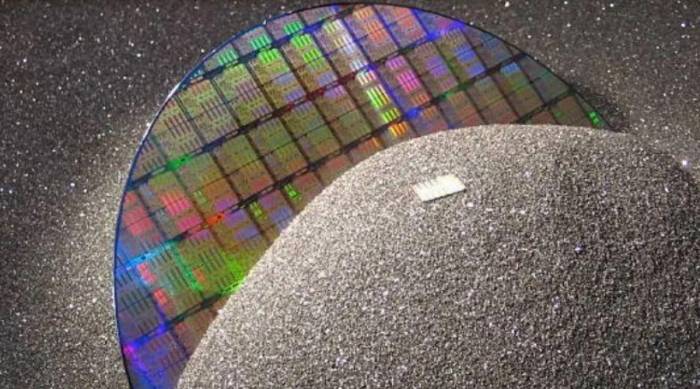
Let's cut straight to the point. No, ASML is not the only photolithography company in the world. That's the simple answer. But if you're reading this, you probably want the messy, complicated, and far more interesting truth. ASML, the Dutch behemoth, dominates the market for the most advanced machines, especially those using Extreme Ultraviolet (EUV) light. Their position is so strong that it's often described as a monopoly in EUV. However, the global photolithography landscape is more like a tiered ecosystem with several other significant players, each holding their ground in specific niches and technologies. Thinking it's just ASML is a common mistake that overlooks a whole world of competition, supply chain dynamics, and strategic alternatives that chipmakers actually use every day.
What You'll Discover in This Guide
The Global Players Beyond ASML
When you step outside the bleeding-edge EUV realm, two Japanese giants immediately come into view: Nikon and Canon. To dismiss them as irrelevant is to misunderstand how most chips are actually made.
Nikon: The Persistent Challenger
Nikon was once the king of lithography. In the early 2000s, they were battling it out with ASML for technological leadership. While they lost the race to develop EUV commercially, they are far from gone. Nikon remains a powerhouse in Argon Fluoride (ArF) immersion lithography. This is the workhorse technology for nodes from about 7nm down to the most advanced non-EUV layers at 5nm and even some 3nm processes.
Here's the thing most people miss: not every layer on a cutting-edge chip requires EUV. Chip designers use a mix of technologies. Many intermediate layers are perfectly served by Nikon's immersion scanners, which are more cost-effective for those steps. Companies like TSMC and Samsung still buy these machines. Nikon's strength lies in precision optics and deep expertise—they just bet on the wrong horse (157nm lithography) 20 years ago, a strategic misstep that allowed ASML to leap ahead with EUV.
Canon: The King of the “Other” Market
If you think Canon only makes cameras and printers, think again. Canon's semiconductor equipment arm, Canon Machinery, is a leader in a completely different segment: i-line, KrF, and lower-end ArF dry lithography. These technologies are used for:
**Mature process nodes:** Think chips for cars, appliances, industrial controllers, and many Internet of Things (IoT) devices. The global chip shortage highlighted the desperate need for capacity in these “legacy” nodes, which are anything but legacy in terms of demand.
**Advanced Packaging:** This is a massive growth area. Technologies like Fan-Out Wafer-Level Packaging (FOWLP) and 2.5D/3D integration use lithography for rerouting layers and silicon interposers. Canon's machines are often the tool of choice here.
**Masks and Reticles:** The photomasks used in all lithography processes are themselves made using specialized lithography systems, and Canon is a key supplier.
Canon's market is enormous in volume. While an ASML EUV machine costs over $150 million, Canon's machines serve a much broader base of fabs worldwide. They dominate by being the reliable, cost-effective solution for the chips that run the physical world.
Why ASML Dominates Advanced Lithography (And It's Not Just the Tech)
ASML's lead in EUV is often attributed to its brilliant engineering. That's true, but it's only half the story. Their real mastery is in system integration and supply chain orchestration.
An EUV machine is arguably the most complex piece of machinery humans have ever built commercially. It doesn't just contain lenses and a light source. It's a fusion of physics, chemistry, materials science, and software. The EUV light source alone, primarily supplied by Germany's Trumpf and Cymer (an ASML company), is a monumental feat—creating plasma by firing lasers at tin droplets in a vacuum.
ASML doesn't make all the critical components. They rely on a hyper-specialized, global ecosystem: Zeiss in Germany for the flawless mirrors, various firms in the US and Japan for sensors and materials. ASML's genius was in recognizing that no single company could do it all, so they became the architect and integrator. They manage this insanely complex supply chain, ensuring all the pieces, each at the limit of known science, work together perfectly.
This creates a moat that's almost impossible to cross. Nikon or Canon couldn't just decide to build an EUV machine tomorrow. They would need to replicate not just the design, but the entire validated ecosystem of suppliers, which is locked in with ASML through years of co-development and billions in joint R&D investment.
The Chinese Challenge: SMEE and the Drive for Self-Sufficiency
This is where geopolitics crashes into technology. Due to export controls, Chinese chipmakers like SMIC cannot buy the latest EUV or even advanced immersion machines from ASML. This has triggered a massive, state-backed push for domestic capability.
The main contender is Shanghai Micro Electronics Equipment (SMEE). Let's be brutally honest about where they stand. SMEE's best commercially available machine is the SSA600 series, which uses 193nm ArF dry lithography. This technology is generations behind ASML's immersion and EUV tools. Reports suggest it's capable of producing chips at the 90nm node, with a push to 28nm being a major national goal.
Progress is slow and fraught with challenges. Building a lithography machine isn't just about copying blueprints; it's about mastering the underlying sciences and building a precision manufacturing culture. The lens systems, the laser stability, the alignment accuracy—these take decades to perfect. While SMEE is making strides (and receiving immense funding), the gap remains vast. They are not a global competitor to ASML today, but they represent a strategic, long-term effort to create an alternative supply chain within China.
Other Chinese companies, like Naura and Advanced Micro-Fabrication Equipment Inc. (AMEC), are also active in adjacent etching and deposition processes, showing a holistic push across the semiconductor equipment sector.
Who Makes What: A Market Segmentation Table
To visualize this tiered market, here’s a breakdown of the key players and their strongholds.
| Company | Key Technology Focus | Typical Application Nodes | Market Position & Notes |
|---|---|---|---|
| ASML (Netherlands) | EUV, High-NA EUV, ArF Immersion | 7nm, 5nm, 3nm, 2nm and beyond | Undisputed leader in advanced logic/foundry. Monopoly in EUV supply. |
| Nikon (Japan) | ArF Immersion, ArF Dry | 45nm to advanced non-EUV layers at 5nm/3nm | Strong #2 in immersion. Critical supplier for memory (DRAM, 3D NAND) and foundry mix-and-match. |
| Canon (Japan) | i-line, KrF, ArF Dry | 350nm to 65nm (mature nodes) | Dominant in mature nodes, advanced packaging, mask making. High-volume, diverse customer base. |
| SMEE (China) | ArF Dry, KrF | 90nm, targeting 28nm | Primary domestic Chinese supplier. Focused on achieving self-sufficiency amid export restrictions. |
Looking at this table, the narrative shifts from "ASML only" to a clear picture of specialization. The semiconductor industry uses the right tool for the right job, and that job isn't always making the latest iPhone processor.
Your Burning Questions Answered
So, is ASML the only photolithography company? Clearly not. They are the undisputed, lonely leader on the highest peak of advanced logic manufacturing. But the mountainside is populated by other strong, vital companies. Nikon competes fiercely on the slopes just below. Canon owns the vast, fertile plains of mature technology and packaging. And new climbers, like SMEE, are attempting the arduous ascent from the base, driven by national necessity.
The health of the global chip industry depends on this diversity. While all eyes are on the peak, the real resilience comes from the entire ecosystem. Understanding that is key to understanding everything from the chip shortage to the future of tech geopolitics.
Comments
Share your experience