According to reports, this CNT film can achieve a high EUV transmission rate of over 92% and a light resistance capability exceeding 1kW exposure output power.
Mitsui Chemicals recently announced that it will begin mass production of semiconductor cutting-edge lithography machine parts (the new generation of thin film materials "Pellicle" that protect the original semiconductor circuits), and plans to set up a carbon nanotube (CNT) film production line at the Iwakuni Otake Plant in Yamaguchi Prefecture, Japan. Mitsui Chemicals expects an annual production capacity of 5,000 sheets, and the production line is expected to be completed in December 2025, which can provide support for the next generation of high numerical aperture, high-output EUV lithography machines to be launched by Dutch ASML.
The next generation of EUV lithography technology has a particularly significant demand for high numerical aperture (NA value 0.55) and high output power (600W and above) processes, and the thin film made of new materials is crucial for withstanding the "harsh lithography environment required to achieve this technology."
For this reason, Mitsui Chemicals has developed a new type of CNT film and decided to mass-produce it. It is reported that this CNT film can achieve a high EUV transmission rate of over 92% and a light resistance capability exceeding 1kW exposure output power.
Mitsui Chemicals hopes to help ASML improve semiconductor performance and productivity by adding a new generation of protective film products using CNT as the film material to its product line, as well as traditional EUV protective films made of silicon-based film.
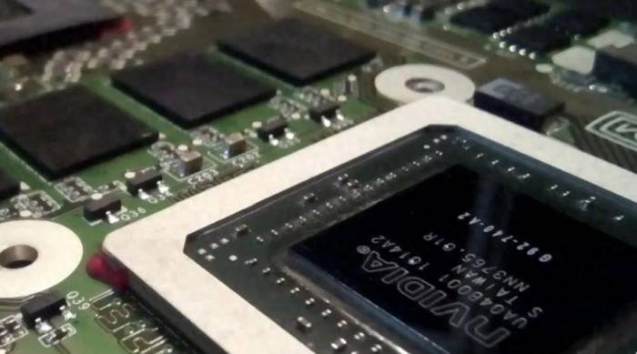
EUV film is key to the yield of 7nm and below chips.Over the past 20 years, light sources, masks, and photoresists have been the three major technical challenges in EUV lithography. More than a decade ago, EUV light sources were usually at the top of the three major technical challenges, and in recent years, with the continuous progress of EUV light sources, EUV masks have begun to take the lead among the three major technical challenges. One of the most difficult aspects of EUV masks is the EUV thin film (Pellicle).
The EUV thin film is an ultra-thin film, a high-end consumable that needs to be replaced regularly, to prevent it from being on the top layer of the EUV mask while allowing high EUV light transmission. It is installed a few millimeters above the surface of the photomask, protecting the surface of the EUV mask from the impact of particles or pollutants in the air during the EUV exposure process. If particles fall on the EUV thin film, due to these particles being out of focus, they will not be exposed on the wafer, thus minimizing exposure defects. However, in the EUV lithography process, EUV light passes through the EUV thin film twice, once incident on the EUV mask, and the other time emitted to the EUV projection optical system, which leads to the temperature of the EUV thin film rising to 600-1000 degrees Celsius.
The EUV thin film protects the extremely expensive 6-inch EUV mask (the cost of a single EUV mask exceeds $300,000) in EUV lithography, keeping it away from particles that may fall on its surface. This is particularly important for the production of CPU chips. The reason is that CPU chips use a single-die mask, and any defect in the EUV mask may cause the entire wafer to fail! If a photomask with 25 bare dies (25-die photomask) is used, it only leads to a 4% reduction in the yield of the entire wafer. In other words, for large-area chips, protection without EUV thin film is absolutely not possible. For small-area chips, protection without EUV thin film may be feasible.
Harry Levinson, the head of HJL Lithography, said: "Trying to perform EUV lithography without an EUV thin film is painful. This requires more inspections, and there is still a risk of yield loss."
Technical challenges and development history of EUV thin films
Joost Bekaert, a researcher at IMEC, the "brain" of European microelectronics, said: "Few materials have a high EUV transmission rate of over 90% while being able to withstand more than 600W of EUV light radiation. In addition, the thin film needs to be strong enough to prevent it on the large area (about 110mm x 140mm) of the EUV mask."
Specifically, EUV thin films must meet the following strict standards:
The thickness is only a few tens of nm (usually 20-30nm), and the large-size thin film corresponds to an area of 110 mm × 140 mm.
In order not to affect the process yield, the transmission rate must be at least more than 90%, and the non-uniformity (3σ) ≤ 0.4%;The EUV (Extreme Ultraviolet) radiation with a high tolerance power density of up to 5W/cm² (corresponding to an EUV power of 400 W);
Strong mechanical properties, with a maximum acceleration of 100 m/s² (corresponding to the movement speed of the thin film on the EUV lithography machine's mask stage), and a Young's modulus exceeding 1 TPa;
Maximum environmental pressure change tolerance of 3.5 mbar/s;
Reflectivity
Lithography technicians have experienced a long and winding journey in the development of EUV thin films. The main reason is that most materials have strong absorption in the EUV band. People have explored various materials such as polysilicon, silicon nitride, carbon nanotubes, and graphene, and there have been many debates on whether EUV lithography must use EUV thin films.
The earliest developers of EUV thin films were ASML company. After efforts, ASML successfully developed a polysilicon EUV thin film with an area of 106 mm × 139 mm in 2014, but its thickness was 70nm, and the highest EUV transmittance was 86%. In 2019, the thickness of the polysilicon EUV thin film was reduced to 50nm, and the highest EUV transmittance was 88%.
In 2019, ASML launched the first commercial EUV thin film and licensed the technology to Japan's Mitsui Chemicals. Mitsui Chemicals began mass sales in the second quarter of 2021. Since then, the debate on whether EUV lithography must use EUV thin films has ended.


Comments
Share your experience