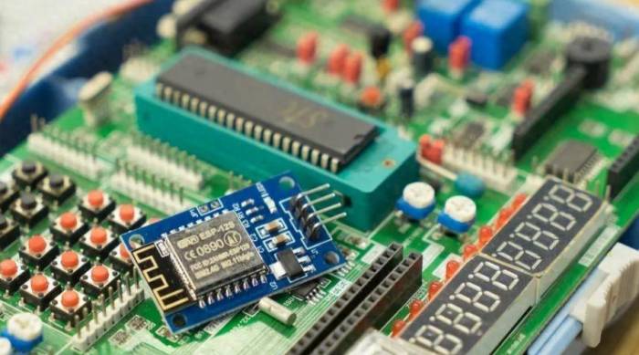
China's domestic semiconductor equipment is gradually reaching its prime.
On June 12th, Huahai Qingke announced that its first 12-inch packaging thinning and lamination machine, Versatile-GM300, was shipped to a leading domestic packaging and testing company.
According to the introduction, the Versatile-GM300 packaging thinning and lamination integrated equipment is another key core product launched by Huahai Qingke in the packaging field following the production model of the thinning and polishing integrated machine (Versatile-GP300) in the advanced packaging field. The machine adopts a new layout throughout, which can flexibly achieve ultra-precision grinding on the back of thin wafers and stress removal of dry polishing. When used in conjunction with a wafer lamination machine, it can provide a full automatic operation process from precision thinning, cleaning and drying to pasting material rings, and stripping back film for 8/12-inch wafers, meeting the production process technology needs of thin wafers in the high-end packaging field.
Huahai Qingke stated that the Versatile-GM300 ultra-precision wafer thinning machine has technically broken through the technical barriers of ultra-thin slice thinning process technology, relying on advanced thickness uniformity control technology, which can achieve in-plane uniformity TTV
Wafer back grinding process
Wafers that have undergone front-end process treatment and wafer testing will start the back-end processing from the back grinding (Back Grinding). Back grinding is a key process, which is not only aimed at reducing the thickness of the wafer, but also effectively solves the problems that may arise between the front and back processes. With the thinning of the thickness of semiconductor chips (Chip), we can achieve more chip stacking (Stacking), thereby improving integration. However, a higher degree of integration may also lead to a decline in product performance, so there is a certain contradiction between integration and product performance. Therefore, choosing the appropriate wafer grinding (Grinding) method is crucial for reducing the cost of semiconductor chips and ensuring product quality.In the semiconductor manufacturing process, the appearance of the wafer undergoes multiple changes. During the wafer fabrication process, we typically polish the edges and surfaces of the wafer, a process that involves grinding both sides of the wafer. After the front-end process is completed, we can proceed with the back-grinding process, which grinds only the back side of the wafer. This step aims to remove the chemically contaminated parts from the front-end process and reduce the thickness of the chip. This is very suitable for manufacturing thin chips mounted on IC cards or mobile devices. In addition, back-grinding also has the advantages of reducing resistance, decreasing power consumption, and improving thermal conductivity to quickly dissipate heat to the back of the wafer. However, due to the thinness of the wafer, it is very susceptible to external forces, making it prone to breakage or warping, making the handling process more difficult.
Back-grinding can generally be divided into the following three steps: First, apply a protective tape lamination to the wafer. Second, grind the back side of the wafer. Finally, before separating the chips from the wafer, the wafer needs to be mounted on a wafer carrier that has a protective tape pre-applied (Wafer Mounting). The wafer carrier process is usually a preparation stage for separating chips (cutting chips) and may be carried out simultaneously with the cutting process. In recent years, as chips continue to become thinner, the process order may also change, and the process steps become more refined.
The first step in back-grinding is to apply the film. Filming is a coating process that pastes the tape onto the front side of the wafer. During the back-grinding process, the silicon compound will diffuse to the periphery of the wafer, and the wafer is also prone to breakage or warping due to external forces, especially when the wafer area is larger, this situation is more likely to occur. Therefore, before back-grinding, we need to apply a thin layer of ultraviolet (UV) blue film to the wafer to protect the surface of the wafer.
During the film application process, to ensure that there are no gaps or bubbles between the wafer and the tape, we need to enhance the adhesion. However, after the back-grinding is completed, to separate the wafer from the tape, we need to reduce the adhesion of the tape by ultraviolet irradiation. After the tape is peeled off, there should be no tape residue left on the surface of the wafer. Sometimes, we can also use a non-ultraviolet de-adhesive film with weaker adhesion and easy to form bubbles, although this method has some shortcomings, but the price is relatively low. In addition, we can also use a bump film that is twice as thick as the UV de-adhesive film, which is expected to be more widely used in the future.
After back-grinding, the thickness of the wafer is usually reduced from 800-700μm to 80-70μm. Reducing the wafer to one-tenth of its thickness can achieve four to six layers of chip stacking. In recent years, through a two-step grinding process, the wafer can even be thinned to about 20μm, thereby achieving a 16 to 32-layer multi-chip packaging (MCP) structure. Although a multi-layer structure is used, in order to ensure that the total height of the finished packaging does not exceed a certain thickness, we still pursue thinner wafers. However, the thinner the wafer, the more inherent defects it has, and the next process will become more difficult. Therefore, we need advanced technology to solve these problems.
The development of back-grinding technology lies in cutting the wafer as thin as possible to overcome the limitations of processing technology. For wafers with a thickness of 50μm or greater, there are usually two steps of rough grinding and fine grinding, after which cutting and polishing and other treatments are carried out. Similar to chemical mechanical polishing (CMP), slurry and deionized water are usually used between the polishing pad and the wafer. This polishing work can reduce the friction between the wafer and the polishing pad, making the surface of the wafer smooth. When the wafer is thicker, ultra-fine grinding can be used, but as the wafer becomes thinner, further polishing is required.
If the wafer becomes thinner, it is prone to external defects during the cutting process. Therefore, for wafers with a thickness of 50μm or less, we can change the process order and adopt the DBG (Dicing Before Grinding) method of cutting first and then grinding. According to the order of dicing, grinding, and dicing again, we can safely separate the chips from the wafer. In addition, there is a special grinding method, which is to use a sturdy glass plate to prevent the wafer from breaking.
With the miniaturization of electronic devices, the requirements for integration are getting higher and higher, and back-grinding technology needs to continuously overcome its limitations and continue to develop. At the same time, we not only need to solve the defects of the wafer itself but also prepare for new process problems that may arise in the future. To cope with these challenges, it may be necessary to readjust the process order, introduce chemical etching technology used in the front-end process of semiconductors, and comprehensively develop new processing methods. To solve the inherent defects of large-area wafers, we are conducting various explorations and experiments to improve the grinding method. In addition, research is also being conducted on how to recycle and utilize the silicon slag produced after grinding the wafer. Through these efforts, we are committed to promoting the advancement of back-grinding technology to meet the needs of the continuously developing electronic industry.

Comments
Share your experience