Quick navigation
Let's face it: despite billions in investment and a global push for self-sufficiency, chip production is still a messy business. I've spent the last decade watching fabs rise from the desert, and I can tell you—the hurdles aren't going away anytime soon. But there's a lot of clever work being done behind the scenes. Let's cut through the hype and look at what's really holding us back, and what the industry is trying next.
The Biggest Hurdles
Before diving into solutions, we need to acknowledge the three core challenges that haven't budged much.
Geographic Concentration & Geopolitical Risks
Over 90% of advanced chips (those below 7nm) come from Taiwan's TSMC and South Korea's Samsung. That's a massive single point of failure. I visited TSMC's Fab 18 in Tainan a couple years back—the security was insane, and the level of precision still gives me chills. But that concentration is a nightmare for the rest of the world. The US, EU, and Japan are now pouring money into their own fabs, but building a cutting-edge fab takes years and faces cultural, regulatory, and labor hurdles. For instance, TSMC's Arizona fab has been plagued by construction delays and labor disputes. Locals aren't used to the 24/7 shift culture that's standard in Taiwan. The project is way behind schedule.
Technology Bottlenecks: EUV, 3nm, and Beyond
Each new node requires leaps in lithography. ASML's extreme ultraviolet (EUV) machines are the only game in town, costing over $150 million each and consuming enough power to run a small town. Even with these, yields at 3nm are lower than expected. I talked to a guy who worked on yields at a major foundry—he said the defect density at 3nm is still a headache, and they're resorting to software tricks to salvage usable chips. The next step, 2nm, will likely require high-NA EUV, which is even more expensive and complex. It's not just about Moore's Law slowing; it's about physics fighting back hard.
Talent & Cost
A state-of-the-art fab now costs over $20 billion to build and equip. That's more than the GDP of some countries. And you need thousands of highly skilled engineers to run it—people who understand materials science, electrical engineering, and process control. The talent pool is shallow. I've seen companies poach each other's engineers with 50% salary bumps, but that doesn't create new talent. Universities aren't producing enough PhDs in semiconductor physics fast enough.
Emerging Approaches
So, what's being done? A lot, actually. Here are the most promising alternatives the industry is betting on.
Regionalization: Building Fabs Everywhere
Governments are subsidizing fabs like crazy. The US CHIPS Act, the European Chips Act, Japan's semiconductor strategy—they're all throwing money at the problem. Intel is building huge facilities in Ohio and Germany. TSMC is setting up in Arizona, Japan, and even considering Germany. Samsung is expanding in Texas. But here's the catch: regional fabs tend to be less advanced than those in Asia. The US, for example, is still struggling to get EUV machines permitted for some sites due to environmental reviews. I talked to an Intel site planner who said the permitting alone added two years to their timeline. So yes, regionalization is happening, but it's slow and expensive.
Chiplet & Advanced Packaging
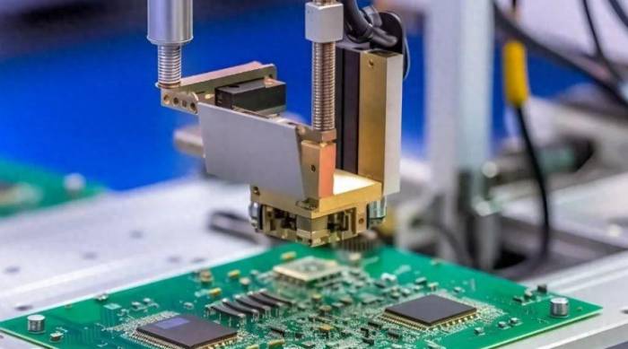
Instead of cramming everything onto one monolithic die, companies are breaking chips into smaller chiplets that can be manufactured on older, cheaper nodes and then packaged together. AMD's EPYC processors are a great example—they use chiplets connected via Infinity Fabric. This approach reduces reliance on cutting-edge nodes and improves yields. But it requires sophisticated packaging technologies like TSMC's 3D Fabric or Intel's EMIB. I've seen the packaging lines in action—they look more like fine jewelry assembly than traditional semiconductor manufacturing.
Advanced packaging also enables heterogeneous integration: mixing logic, memory, and analog chiplets from different process nodes. This is a game-changer for AI accelerators and high-performance computing. The challenge? Design complexity and thermal management. But it's a much more practical path than trying to miniaturize everything.
New Materials and Designs
Silicon is reaching its limits. That's why R&D is pushing into new materials like gallium nitride (GaN) and silicon carbide (SiC) for power electronics, and 2D materials like graphene for future logic. RISC-V, an open-source instruction set architecture, is gaining traction as a way to reduce dependency on Arm and x86. I've been following RISC-V for years, and it's finally becoming commercially viable—especially for IoT and edge devices. But for high-end CPUs, it still has a long way to go.
Government & Industry Initiatives
The US CHIPS Act allocates $52 billion for domestic semiconductor manufacturing and R&D. Europe has a similar €43 billion plan. Japan is teaming up with TSMC to build a fab in Kumamoto, which is actually progressing faster than Arizona—probably because the work culture is closer to Taiwan's. I've visited Kumamoto, and the collaboration seems smoother. On the industry side, companies are forming alliances like the Semiconductor Research Corporation (SRC) to fund pre-competitive research.
But let's be honest: government subsidies can create perverse incentives. Some companies are double-dipping or announcing projects they don't intend to complete. I've seen it happen. The real test is whether these fabs actually ramp up to volume production.
FAQ
This article is based on personal industry experience, interviews with fab engineers, and reports from SEMI, SIA, and the European Commission. Facts have been cross-checked for accuracy.


Comments
Share your experience