As chip sizes increase, the capacity of 12-inch wafers is gradually becoming insufficient.
TSMC is researching a new advanced chip packaging method that uses a rectangular substrate instead of the traditional circular wafer. According to reliable sources, TSMC's rectangular substrate is currently in a rigorous testing phase. Its dimensions reach 510mm x 515mm, which, compared to the size of a 12-inch wafer, this innovative design significantly increases the usable area of the substrate compared to the circular wafer, by more than three times, allowing for more chips to be placed.
Moreover, the new substrate also helps to reduce waste in the production process, further improving manufacturing efficiency.
Although this research is still in its early stages, it has already faced a series of technical challenges. Especially when packaging cutting-edge chips on the new-shaped substrate, the application of photoresist has become a key bottleneck. This requires chip manufacturing giants like TSMC to leverage their deep financial advantages to promote equipment manufacturers to innovate in equipment design.
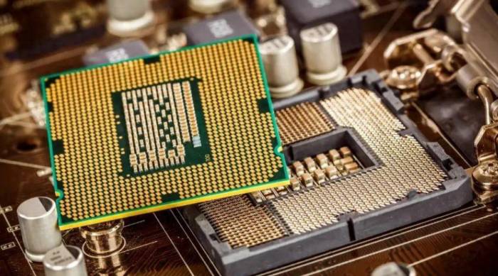
In the current wave of technology, AI servers, high-performance computing (HPC) applications, and high-end smartphone AI are continuously driving the development of the semiconductor industry. Against this backdrop, TSMC's 3-nanometer family process capacity has become a hot focus in the market. It is reported that its capacity is already in short supply, and the customer queuing phenomenon has continued until 2026.
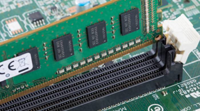
Currently, the AI chips produced by TSMC for companies such as Nvidia, AMD, Amazon, and Google use 12-inch silicon wafers, which is the largest wafer size available. However, with the increase in chip size, the capacity of 12-inch wafers is gradually becoming insufficient. According to Morgan Stanley's estimates, the earlier H200 and H100 chips can be packaged into about 29 sets on a single wafer, while only 16 sets of B200 can be manufactured on a 12-inch wafer, and this is still under the ideal condition of a production yield rate of 100%.What Prevents the Production of Chips on 18-inch (450mm) Wafers?
Driven by Moore's Law, production costs have been continuously decreasing, which has also brought about technological innovations. To improve the production efficiency and profitability of products, the expansion of wafer size and the reduction of chip linewidth are the two main threads of technological progress in the integrated circuit industry.
Generally speaking, the semiconductor industry upgrades its fab architecture every decade to increase the wafer diameter, while the process technology maintains a pace of one node every two years. As the nanoscale approaches the physical limit, the progress of process nodes has slowed down, and the increase in wafer size has become more and more important.
The larger the wafer size, the more chips can be manufactured on each wafer, thus the manufacturing cost is lower. Wafer sizes have evolved from the early 2-inch (50mm), 4-inch (100mm), to 6-inch (150mm), 8-inch (200mm), and 12-inch (300mm), with an upgrade approximately every 10 years.
Currently, more than 70% of the world's chip production capacity is on 12-inch (300mm) wafers, and the first 12-inch Fab line has been in operation for nearly twenty years. Why haven't we seen the next generation of 18-inch (450mm) wafer fabs yet?
Research and Development Costs
When discussing the main challenges of 18-inch wafers, the first issue is their enormous cost. Although 450mm wafers can reduce the cost per die, achieving this goal is not easy. It is estimated that the transition from 150mm to 200mm cost nearly 1.5 billion USD; and from 200mm to 300mm, it invested 11.6 billion USD, with the cost increasing by almost eight times. Advancing to the 450mm scale will require more than 100 billion USD in research and development costs.
Time and Equipment Costs
The equipment and time costs required for wafer size migration have slowed the pace of progress. Although the area of a 450mm wafer is more than twice that of a 300mm wafer, the production time far exceeds twice. SEMI once predicted that each 450mm wafer fab would cost 10 billion USD, but the cost per unit area of chips would only decrease by 8%. This high financial pressure and the unclear improvement in efficiency have led the industry to slow down the pace of transitioning to the 450mm process.
Low Yield RatesYield rate is also a huge challenge. The larger the wafer size, the higher the requirements for the process, equipment, and materials. The unpredictability of the yield rate increases the risk. The larger the wafer diameter, the higher the wafer utilization rate and the greater the number of chips. However, in practical applications, because about 75% of silicon wafers are produced by the Czochralski method, the larger the diameter, the greater the possibility of lattice structure defects due to unstable rotation speed during the crystal growth process. Therefore, when the cost reduction achieved by increasing the wafer size cannot compensate for the increased cost of wafer defects caused by large diameters, it becomes uneconomical to choose larger wafers for production.
TSMC gives up on 18-inch wafers
Due to various limiting factors, TSMC, which once seriously promoted 18-inch wafers, gradually lost enthusiasm. Chiang Shang-Yi recalled a meeting with Morris Chang, who said that TSMC should not develop 18-inch wafers. TSMC's main competitors in 12-inch wafers are UMC, SMIC, etc., all of which are smaller in scale than TSMC, and these companies' capital cannot be compared with TSMC, giving TSMC more leading advantages. However, the competitors for 18-inch wafers would be Intel, Samsung, etc., these large factories have strong capital and more sources of income than TSMC, and the investment amount is higher than TSMC. If so, TSMC would lose its competitive advantage and would go from being a big fish in a pond to a small fish in the ocean. Morris Chang had more than 10 meetings with Chiang Shang-Yi, and finally, TSMC decided not to continue the development of 18-inch wafers.
During the 2013 SEMICON West Semiconductor Conference held by TSMC, there was a closed-door meeting with Intel, Samsung, TSMC, and equipment manufacturers such as ASML. TSMC synchronized this decision with other companies. Chiang Shang-Yi said that TSMC will only develop advanced processes and no longer develop 18-inch wafers.


Comments
Share your experience