If you're holding a smartphone, using a laptop, or driving a modern car, you're interacting with products built around chips made possible by photolithography. And when we talk about the pinnacle of this technology, one name dominates the conversation completely: ASML Holding N.V. This Dutch company isn't just a player; it's the sole supplier of the most advanced photolithography machines on the planet. Their extreme ultraviolet (EUV) lithography systems are so complex and critical that they've become a geopolitical asset. Let's cut through the noise. This isn't about a generic "specialist." It's about understanding how ASML built a fortress-like monopoly and why that matters to every tech product you buy.
In This Article
Why Photolithography is the Make-or-Break Step
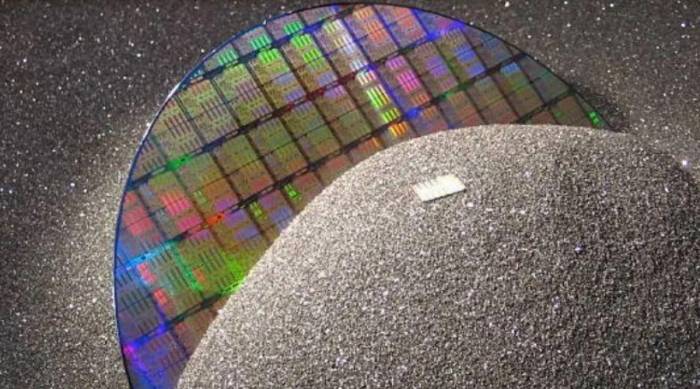
Think of building a chip like printing a microscopic city. Photolithography is the process that "prints" the intricate circuit patterns onto silicon wafers. The wavelength of light used determines how fine these patterns can be. Smaller wavelengths mean smaller, faster, and more efficient transistors. It's the fundamental bottleneck in Moore's Law.
The jump to extreme ultraviolet light (EUV), with a wavelength of 13.5 nanometers, was the industry's moonshot.
It took decades and billions in R&D. Every major chipmaker—Intel, TSMC, Samsung—knew they needed it to make chips at 7nm nodes and below. But only one company could deliver a working, high-volume production tool. That company was ASML.
The Core Challenge: It's not just about generating EUV light. It's about generating it powerfully enough (a plasma created by firing a laser at tin droplets), in a perfect vacuum (because air absorbs EUV), and directing it with mirrors so smooth that if they were expanded to the size of Germany, the largest imperfection would be a millimeter high. ASML mastered this physics nightmare.
How ASML Achieved Total Dominance
ASML's lead isn't an accident. It's the result of a brilliant and risky strategy executed over 30 years. In the 1980s and 90s, the photolithography market was a fight between US, Japanese, and Dutch companies. ASML, spun out from Philips, was an underdog.
Their masterstroke was embracing an "open innovation" model. Instead of trying to build every component in-house, they acted as the supreme systems integrator. They identified the world's best specialists for lenses (Zeiss from Germany), light sources (initially Cymer, now fully owned), and stages (precision movers), and forged deep, exclusive partnerships. They got their key customers—Intel, Samsung, TSMC—to invest directly in their R&D, creating a financial and feedback loop that locked in demand.
When the EUV bet looked shaky in the 2000s, ASML doubled down while competitors like Nikon scaled back. They turned a scientific challenge into an engineering production problem. Today, that bet pays over €20 billion in annual revenue.
The Financial and Market Reality
Let's look at the numbers. The table below shows why "specializes" is an understatement for ASML in the high-end segment.
| Company | Key Technology | Market Share (Immersion & EUV) | Approx. System Cost | Primary Customers |
|---|---|---|---|---|
| ASML | EUV, High-NA EUV, Immersion DUV | >90% for advanced nodes | €150M - €350M per system | TSMC, Intel, Samsung, SK Hynix |
| Nikon | Immersion DUV, ArF Dry | €10M - €50M | Smaller fabs, specialty ICs | |
| Canon | i-line, KrF DUV | Minor (mature nodes) | Display, MEMS, power devices |
You see the gap. An ASML EUV machine costs more than a Boeing 787 Dreamliner and is exponentially more complex. Customers wait years for delivery. This isn't just specialization; it's a captive market.
Inside the EUV Machine: A Technical Marvel
To appreciate the monopoly, you need to grasp what's inside those shipping-container-sized machines. An EUV scanner is a symphony of impossible engineering.
The Light Source: A high-power laser fires at 50,000 microscopic tin droplets per second, creating a plasma that emits the 13.5nm EUV light. The power target for years was 250 watts at the intermediate focus—a milestone that seemed unreachable. ASML's persistent iteration got them there, enabling wafer throughput that makes economic sense for fabs.
The Optics: All lenses absorb EUV light. So the entire system uses only mirrors. Zeiss manufactures these multi-layer mirrors, stacking thousands of alternating silicon and molybdenum layers with atomic-scale precision. The mirror surfaces are the smoothest objects ever made by humans. Contamination is the enemy; a single dust particle can ruin a mirror worth millions.
The Environment: The entire light path is in a near-perfect vacuum because air molecules absorb EUV. The wafer stage moves the silicon wafer with nanometer precision while accelerating faster than a fighter jet. It's a ballet of extreme physics happening hundreds of wafers per day.
The Ecosystem and Supply Chain Lock-in
Here's a subtle point most analyses miss: ASML's dominance is protected by its supply chain. They don't just have patents; they have relationships.
Take Zeiss. They've co-evolved with ASML for decades. Their mirror technology is so specialized it has no other commercial application at this scale. Building a competitor would require not just replicating ASML but also replicating Zeiss, and Cymer's source technology, and the half-dozen other single-source suppliers. You'd need to reassemble a globally distributed, decades-deep knowledge network. That's a taller order than the tech itself.
Furthermore, ASML's machines are now deeply integrated into the process flows at TSMC, Intel, and Samsung. Chip designs are optimized for ASML's scanner characteristics. Switching would require redesigning chips and processes—a multi-billion dollar setback no fab can afford.
The Rest of the Field: Nikon and Canon
It's important to note that ASML doesn't make every lithography tool. Japanese giants Nikon and Canon are still significant companies that specialize in photolithography, but for different segments of the market.
Nikon remains a strong competitor in deep ultraviolet (DUV) immersion lithography, which is used for chips at nodes from about 40nm down to 7nm (where EUV takes over). Their systems are excellent and critical for many chip types—memory, sensors, and many automotive chips don't yet require EUV. However, they've publicly conceded the EUV race to ASML for now.
Canon dominates the lower-end, higher-volume market for older "i-line" and "KrF" lithography. These machines are workhorses for manufacturing displays, micro-electro-mechanical systems (MEMS), and power semiconductors. They're reliable, much cheaper, and vital for the Internet of Things (IoT) ecosystem.
So, the landscape is tiered.
ASML owns the cutting-edge frontier. Nikon holds the vital advanced-DUV middle ground. Canon owns the mature, high-volume base. But the direction of travel—toward ever-smaller features—flows through ASML's EUV and next-gen High-NA EUV tools.
What This Means for Chip Design and Supply
ASML's position creates both stability and vulnerability for the global tech supply chain.
For Chip Designers: Your architectural choices are implicitly bounded by what ASML's machines can print. Designing for manufacturability (DFM) means designing for ASML's quirks and capabilities. This centralizes immense power. A delay in ASML's next-generation High-NA EUV rollout could delay entire generations of CPUs and GPUs across multiple companies.
For Geopolitics: ASML has become a geopolitical tool. Export controls on its machines to certain regions are a primary lever in tech wars. This puts ASML in a difficult position—it's a Dutch company with a global supply chain caught between superpowers. The recent restrictions highlighted that access to ASML's technology is now a matter of national industrial policy.
For Startups and Innovation: It creates a massive barrier to entry. You can't start a leading-edge foundry without ASML's blessing and a place in its multi-year backlog. This concentrates advanced manufacturing in the hands of three or four giant fabs. Innovation in chip *design* flourishes (think AI accelerators), but innovation in chip *manufacturing* is incredibly centralized.
Expert Insights: Your Burning Questions Answered
Can any company, like China's SMEE, realistically catch up to ASML in EUV?
The short-term answer is no, and the long-term answer is extraordinarily difficult. Catching up isn't about copying one machine; it's about replicating an entire ecosystem of sub-component suppliers that took 30 years to cultivate. Reports from analysts at institutions like SEMI suggest that even with intense investment, a competitor would be years behind in reliability and throughput—the metrics that actually matter in a fab. The knowledge isn't just in blueprints; it's in the tacit experience of thousands of engineers solving problems that only appear after years of machine operation.
If I'm an engineer, what part of ASML's technology is the most underrated career niche?
Most people look at optics or the light source. I'd argue it's systems integration and data analytics. Making 100,000 precision parts work together is one thing. Using sensor data from every machine in the field to predict failures, optimize performance, and guide the design of the next generation is where the real secret sauce is now. ASML's deep fleet data is an insurmountable advantage. Engineers who can bridge hardware physics with big data and machine learning are the unsung heroes keeping the yield high.
What does ASML's dominance mean for the cost and availability of future chips?
It creates a paradox. On one hand, the astronomical R&D and machine costs (the next-gen High-NA EUV tool may approach $400 million) contribute to the rising price of building fabs, which is in the tens of billions. This cost is amortized over billions of chips, but it still pushes the industry toward consolidation. On the other hand, without ASML's machines, we simply wouldn't have advanced chips at all—cost would be infinite. Their continued innovation is what keeps Moore's Law on life support, providing more transistor density per dollar. The risk isn't price; it's resilience. A fire at one key supplier in ASML's chain could halt production of all advanced lithography tools globally.
Are there any alternative technologies that could bypass EUV lithography altogether?
Research is always ongoing. Nanoimprint lithography (NIL), championed by Canon, is a dark horse. It's like a microscopic stamp, potentially cheaper and simpler. But it has struggled for decades with defect rates and overlay accuracy at the scales needed for complex logic chips. It may find a home in memory chips or photonics first. Directed self-assembly (DSA) is another lab curiosity. The reality is that EUV, and specifically ASML's implementation of it, has won the race for the foreseeable next decade. The industry has bet trillions of dollars on this roadmap. Any alternative would need to be not just slightly better, but astronomically better to justify the monumental switch in infrastructure and design rules.


Comments
Share your experience