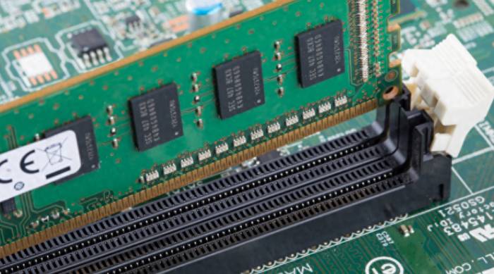
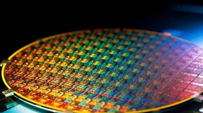
Despite the significant slowdown in the pace of Moore's Law, the process nodes continue to move forward steadily, now evolving to below 2nm or even 1nm. In the latest logic nodes, the traditional device architecture no longer has an advantage, and the Complementary Field-Effect Transistor (CFET) is regarded as a "big player," becoming the mainstream architecture of the era of Angstrom (1 Angstrom equals 0.1 nanometers). So, what exactly is the charm of CFET?
01
Why is CFET needed?
CFET, as an innovative CMOS process, breaks through the limitations of traditional planar processes, FinFET (Fin Field-Effect Transistor), and GAAFET (Gate-All-Around Field-Effect Transistor) with its unique vertical stacking of transistors.
Why is the CFET architecture highly regarded? Let's take a look at the bottlenecks faced by FinFET and GAAFET under current technical challenges, and it is not difficult to understand why CFET is worth in-depth research.
First, let's look at FinFET.
FinFET is a new type of complementary metal-oxide-semiconductor (CMOS) transistor, and the inventor of this technology is Professor Chenming Hu from the University of California, Berkeley.
In 2011, Intel was the first to commercialize FinFET technology and applied it to the 22nm process, significantly improving performance and reducing power consumption. Subsequently, manufacturers such as TSMC and Samsung followed suit, and FinFET technology shone brightly. Later, to improve transistor performance and further reduce area, the FinFET architecture also underwent continuous improvements. Since the 16/14nm node, FinFET has become the mainstream choice, driving the development of semiconductor processes to the 3nm node. However, in reality, since entering the 5nm node, FinFET has started to face challenges such as fin stability, gate width limitations, and electrostatic issues. The patched-up FinFET will eventually be unable to cope, and a new architecture is thus urgently needed.The next contender in line is the GAAFET. GAAFET stands for Gate-All-Around Field-Effect Transistor, and its fundamental structure involves rotating the Fin of the FinFET by 90 degrees and then stacking multiple Fins horizontally, all of which pass through the gate.
There are two types of GAAFET structures: one that uses nanowire as the fin of the electronic transistor, and the other is a multi-bridge channel field-effect transistor (MBCFET) with thicker fins in the form of nanosheets.
It is reported that Samsung has already introduced the GAAFET architecture at the 3nm process node, while TSMC will first apply GAAFET transistors at the 2nm process node, and Intel previously stated that it will introduce RibbonFET transistor architecture with GAA design in the Intel 20A process.
With the GAAFET transistor, the contact area between the gate and the channel increases, and while the width of the Fin is a fixed value for FinFET, for GAAFET, the width of the sheet itself and the effective channel width are flexible and variable. A wider sheet naturally achieves higher driving current and performance, while a narrower sheet occupies less area and naturally provides better electrostatic characteristics than FinFET, meeting the requirements of some gate widths.
Under the same size structure, the channel control ability of GAAFET is enhanced, further miniaturization is more possible, and the production process required for the new structure should be similar to that of the fin transistor, allowing the use of existing equipment and technical achievements.
However, although GAAFET has been implemented in 3nm and even 2nm processes, further scaling down to below 1nm will face huge process challenges.
At this point, the industry's technology giants have begun to adjust their strategies, focusing their attention and efforts on the emerging technology of CFET.
02
CFET Shows Its StrengthCFET integrates GAA devices with different conductive channel types (N-FET and P-FET) in a high-density three-dimensional monolithic vertical configuration. Compared to the mainstream FinFET and GAAFET transistor integrated circuit processes currently in use, CFET breaks through the size limitations of the traditional N/P-FET co-planar layout spacing, allowing the logic standard cell size in integrated circuits to be shrunk to a height of 4-T (Track), while reducing the SRAM cell area by more than 40%. In the field of future technology that pursues ultimate performance and density, CFET will undoubtedly become a strong candidate for innovative architectures of basic transistor devices.
At the 2023 IEEE International Electron Device Conference, TSMC released a paper titled "Complementary Field-Effect Transistors (CFETs) with 48-nm Gate Pitch for Future Logic Technology Scaling," whose devices are distinguished by a new method of forming a dielectric layer between the top and bottom devices to maintain their isolation. Nanowires are generally formed by alternating silicon and silicon-germanium layers. At the appropriate steps in the process, the specific etching method of silicon-germanium will remove these materials, thereby releasing silicon nanowires. TSMC uses silicon-germanium layers to isolate the two devices, knowing that the etching speed of the silicon-germanium layer is faster than other silicon-germanium layers, so a silicon-germanium layer with a particularly high germanium content is used. In this way, the isolation layer can be made in several steps before the release of the silicon nanowires.
Recently, TSMC Senior Vice President and Co-Chief Operating Officer Zhang Xiaoqiang announced at the 2024 Technology Forum that TSMC has successfully integrated different transistor architectures and made CFET in the laboratory. Zhang Xiaoqiang pointed out that CFET is expected to be introduced into the next generation of advanced logic processes. CFET is the next brand-new transistor architecture after the nanosheet field-effect transistor architecture adopted by the 2nm process.
Not only TSMC but also the three chip giants including Samsung and Intel attach great importance to the development of CFET.
Intel was the first among the three to demonstrate CFET, releasing an early version at IEDM as early as 2020, and then making several improvements around the simplest CFET circuit (inverter) at the 2023 IEEE International Electron Device Conference. Marko Radosavljevic, Chief Engineer of Intel's Component Research Group, said: "The inverter is completed on a single fin. At the maximum scaling ratio, it will be 50% of the size of a conventional CMOS inverter." In addition, Intel also increased the number of nanowires per device from 2 to 3 and reduced the spacing between the two devices from 50 nm to 30 nm.
Samsung is also very active in the development of CFET. At last year's IEEE conference, Samsung demonstrated the results of 48nm and 45nm contact poly silicon spacing (CPP). However, these results were for individual devices, not complete inverters. Although the performance of the smaller of Samsung's two prototype CFETs has declined, the extent is not large, and the company's researchers believe that manufacturing process optimization will solve this problem.
The key to Samsung's success is the ability to electrically isolate the sources and drains of the stacked pFET and nFET devices. Without sufficient isolation, the device, known as the three-dimensional stacked field-effect transistor (3DSFET) by Samsung, will leak current. The key step in achieving this isolation is to replace the etching step involving wet chemicals with a new type of dry etching. This has increased the yield of good devices by 80%.
Like Intel, Samsung also contacts the bottom of the device from below the silicon wafer to save space. However, the difference between this South Korean chip manufacturer and the American company is that it only uses one nanowire in each paired device, instead of Intel's three. According to its researchers, increasing the number of nanowires will improve the performance of CFET.Of course, in addition to the chip industry's top three, companies and research institutions from other countries and regions are also actively participating in the development and research of CFETs.
As early as around the year 2000, Peking University had already proposed the concept of three-dimensional stacked complementary metal-oxide-semiconductor (CMOS) transistors, and by 2004, they had developed a prototype of the stacked CMOS transistor, publishing the paper "A stacked CMOS technology on SOI substrate." They also applied for the patent "A CMOS circuit structure located on an SOI substrate and its manufacturing method" as the first patent holder in China. However, this concept was too advanced at the time and did not attract much attention.
In recent years, this paper and its subsequent work have been cited hundreds of times in international invention patents and have been highly praised by industry giants. In the IEDM 2021 conference, Intel's invited talk on transistor stacking technology, "Opportunities in 3-D stacked CMOS transistors," cited the aforementioned paper, which was the earliest cited document; TSMC pointed out in its VLSI 2021 report, "CMOS Device Technology for the Next Decade," that Peking University's 3D stacked CMOS transistor was the industry's first stacked complementary transistor, predating TSMC and Intel by 15 years.
At IEDM 2021, the Institute of Microelectronics at Peking University published a paper titled "Demonstration of Vertically-Stacked CVD Monolayer Channels: MoS2 Nanosheets GAA-FET with Ion>700μA/μm and MoS2/WSe2 CFET," showcasing a stacked gate-all-around nanosheet device based on molybdenum disulfide monolayers, achieving an on-state current of over 400μA/μm (at Vd=1V) or 700μA/μm (at Vd=2V), far exceeding the reported levels of similar devices in the literature. Through statistical analysis of hundreds of devices, the performance improvement brought by three-dimensional integration and size reduction was demonstrated. For the first time, a CFET device with a channel thickness of less than 1 nanometer, made of molybdenum disulfide/tungsten diselenide, was reported, achieving the logic function of an inverter.
The Institute of Microelectronics of the Chinese Academy of Sciences has also made certain progress in the research of CFET structure design and simulation. In July 2022, the research team of Yin Huaxiang/Wu Zhenhua from the Leading Process R&D Center of Integrated Circuits at the Institute of Microelectronics of the Chinese Academy of Sciences used the industry's mainstream Design-Technology Co-optimization (DTCO) method to fully explore the advantages of CFET device architecture, proposing a new hybrid channel complementary FET (Hybrid Channel Complementary FET, HC-CFET) structure design and integration scheme. This structure can achieve co-optimization of the preferred high electron and hole mobility conductive channels for N-FET and P-FET on a single substrate, without the need for hybrid crystal orientation technology such as wafer bonding, by using the high etching selectivity ratio of SiNx and SiO2 and step-by-step channel morphology etching, making N-FET have a (100) channel surface crystal orientation and P-FET have a (110) channel surface crystal orientation, thereby obtaining the best device and circuit performance under the same projection plane. The feasibility of this structure design and integration scheme has been verified by Virtual-FAB simulation. Further, by accurately solving all parasitic parameters, the performance of 17-stage ring oscillators and SRAM cells under different CFET architectures was compared. The results show that compared with conventional vertical integrated Fin and vertical integrated nanosheet CFET structures (MS-CFET and MB-CFET), the new HC-CFET has channel crystal orientation and spatial layout advantages, showing higher operating frequencies and better noise margin windows, as well as great potential in high-performance CMOS integrated circuit applications with high miniaturization. This achievement was published in the journal "IEEE Transactions on Electron Devices" (IEEE Transactions on Electron Devices 69, 3581 (2022), DOI: 10.1109/TED.2022.3176843) with the title "Investigation of Novel Hybrid Channel Complementary FET Scaling Beyond 3-nm Node From Device to Circuit."
In December 2022, Nature Electronics published a paper by the Microelectronics College of Fudan University titled "Heterogeneous Complementary Field-effect Transistors Based on Silicon and Molybdenum Disulfide." The team introduced a new type of two-dimensional atomic crystal into the traditional silicon-based chip manufacturing process, achieving wafer-level heterogeneous CFET technology. Compared with silicon materials, the atomic layer precision of two-dimensional atomic crystals gives them superior short-channel control capabilities in small-sized devices. Using the standard back-end process of silicon-based integrated circuits, the new two-dimensional material MoS2 was three-dimensionally stacked on traditional silicon-based chips, and the highly matched physical properties of the two were used to form a p-type silicon-n-type MoS2 heterogeneous CFET structure. The integration density of integrated circuits was doubled under the same process node, and superior device performance was obtained.
03
When will 1nm arrive?Tom's Hardware reports that Intel confirmed at a closed-door event during the IFS Direct Connect conference that, according to current plans, the "meaningful" scale production of the 14A node will fall in 2026; while the next process node, 10A, which has not yet been officially announced, is expected to start production by the end of 2027.
TSMC recently unveiled its product roadmap for advancing to the 1nm process at the 2023 IEEE International Electron Devices Meeting (IEDM). According to the plan, TSMC will simultaneously promote the development of 3D packaging and single-chip packaging technology paths. It is expected that by 2025, TSMC will complete the N2 and N2P nodes, enabling chips using 3D packaging to have more than 50 billion transistors, while chips using traditional packaging technology will have more than 10 billion transistors.
Then, TSMC plans to reach the A14 node in 2027 and the A10 node, that is, the 1nm process chip, by 2030. At that time, the number of transistors in chips using TSMC's 3D packaging technology will exceed 100 billion, while the number of transistors in chips using traditional packaging technology will exceed 20 billion.
IBM has always been a leader in semiconductor technology innovation. In 2021, IBM announced the launch of the world's first 2nm chip. At the same time, IBM also started researching 1nm technology early on. At the end of 2022 IEDM conference, IBM demonstrated its technology prepared for the path to 1nm and beyond: Interconnect 3.0 and VTFET.
In 2022, Japanese chip manufacturer Rapidus, the University of Tokyo, and the French semiconductor research institution Leti will cooperate to jointly develop 1nm process semiconductors. This cross-country cooperation model provides a new perspective and resources for technological innovation, which is expected to accelerate the development process of 1nm technology.
In May 2023, Imec released its roadmap for transistors below 1nm, showing the possible path and technical difficulties for achieving the 1nm process in the next few years. Imec is committed to developing products that far exceed the limits of existing technology. Subsequently, in June, IMEC also reached an agreement with ASML to strengthen cooperation in the next phase of developing the most advanced high numerical aperture (High-NA) extreme ultraviolet (EUV) lithography test line, providing a prototype design platform and undeveloped future opportunities for the industry using semiconductor technology.
IMEC CMOS Director Naoto Horiguchi said in a speech at the International Electron Device Meeting: "It is very difficult to scale CMOS devices using GAA alone. With CFET, we can continue to extend the devices, and then we can combine it with other technologies such as Chiplet and advanced packaging to improve chip performance. CFET is paving the way for the continued extension of devices." IMEC expects that the CFET architecture will surpass the 1nm node around 2032.
However, it is worth noting that there are still many problems facing CFET, especially in the future mass production process, the manufacturing of CFET will be more difficult. On the one hand, the CFET architecture has a higher 3D structure than the GAA architecture, and the increase in the aspect ratio of the structure will bring greater manufacturing challenges; on the other hand, CFET requires very high dopant activation, very low contact resistivity, and special high-k/metal gates for CFET, and all of this must be completed in a very high stacking structure.
TSMC said that the significant challenges of the CFET architecture may lead to increased process complexity and cost. "To overcome these challenges, it is necessary to carefully choose the integration scheme to reduce process complexity and minimize the requirements for new materials and process capabilities." TSMC Device Architecture Development Director Szuya Liao said, "It is also important to participate in early EDA/process tool development and prepare for major design changes."


Comments
Share your experience